Before we begin
Today we’ll be looking into the NVIDIA GeForce xx70 line of graphics cards to see how much they’ve upgraded and improved through the years, as well as the transition from GTX to RTX and the introduction of ray tracing.
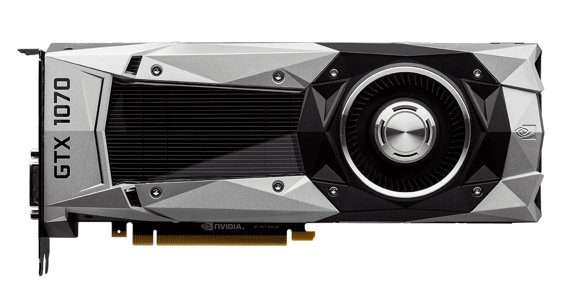
NVIDIA GeForce GTX 1070

Graphics Processor
GPU Name: GP104
GPU Variant: GP104-200-A1
Architecture: Pascal
Foundry: TSMC
Process Size: 16 nm
Transistors: 7,200 million
Die Size: 314 mm²
Graphics Card
Release Date: Jun 10th, 2016
Generation: GeForce 10
Predecessor: GeForce 900
Successor: GeForce 20
Production: End-of-life
Launch Price: $379 USD
Bus Interface: PCIe 3.0 x16
Clock Speeds
Base Clock: 1506 MHz
Boost Clock: 1683 MHz
Memory Clock: 2002 MHz, 8 Gbps effective
Memory
Memory Size: 8 GB
Memory Type: GDDR5
Memory Bus: 256 bit
Bandwidth: 256.3 GB/s
Slot Width: Dual-slot
Length: 267 mm, 10.5 inches
Width: 112 mm, 4.4 inches
Height: 40 mm, 1.6 inches
TDP: 150 W
Suggested PSU: 450 W
Outputs: 1x DVI, 1x HDMI 2.0, 3x DisplayPort 1.4a
Power Connectors: 1x 8-pin
Board Number: PG411 SKU 20
Graphics Features
DirectX: 12 (12_1)
OpenGL: 4.6
OpenCL: 3.0
Vulkan: 1.3
CUDA: 6.1
Shader Model: 6.4
Render Config
Shading Units: 1920
TMUs: 120
ROPs: 64
SM Count: 15
L1 Cache: 48 KB (per SM)
L2 Cache: 2 MB
Theoretical Performance
Pixel Rate: 107.7 GPixel/s
Texture Rate: 202.0 GTexel/s
FP16 (half) performance: 101.0 GFLOPS (1:64)
FP32 (float) performance: 6.463 TFLOPS
FP64 (double) performance: 202.0 GFLOPS (1:32)
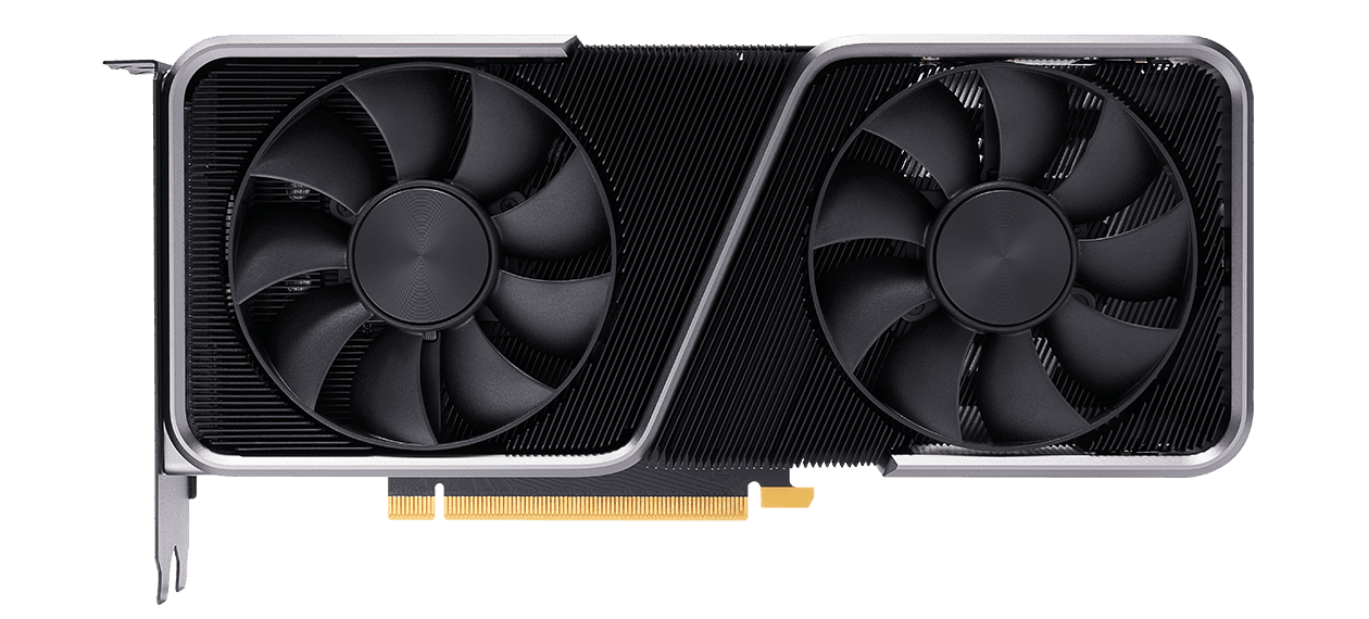
NVIDIA GeForce RTX 2070
The 20 series is where we see the introduction to RTX. NVIDIA’s transition from GTX to RTX was a huge stepping stone for more realistic graphics as real-time tracing was able to simulate individual rays of light. RTX graphics cards also established Tensor cores which are used to accelerate deep learning which allows users to upscale their resolution without a significant loss of performance.

Graphics Processor
GPU Name: TU106
GPU Variant: TU106-400A-A1
Architecture: Turing
Foundry: TSMC
Process Size: 12 nm
Transistors: 10,800 million
Die Size: 445 mm²
Graphics Card
Release Date: Oct 17th, 2018
Generation: GeForce 20
Predecessor: GeForce 10
Successor: GeForce 30
Production: Active
Launch Price: $499 USD
Bus Interface: PCIe 3.0 x16
Clock Speeds
Base Clock: 1410 MHz
Boost Clock: 1620 MHz
Memory Clock: 1750 MHz, 14 Gbps effective
Memory
Memory Size: 8 GB
Memory Type: GDDR6
Memory Bus: 256 bit
Bandwidth: 448.0 GB/s
Board Design
Slot Width: Dual-slot
Length: 229 mm, 9 inches
Width: 113 mm, 4.4 inches
Height: 35 mm, 1.4 inches
TDP: 175 W
Suggested PSU: 450 W
Outputs: 1x DVI, 1x HDMI 2.0, 2x DisplayPort 1.4a, 1x USB Type-C
Power Connectors: 1x 8-pin
Board Number: PG160 SKU 52
Graphics Features
DirectX: 12 Ultimate (12_2)
OpenGL: 4.6
OpenCL: 3.0
Vulkan: 1.3
CUDA: 7.5
Shader Model: 6.6
Render Config
Shading Units: 2304
TMUs: 144
ROPs: 64
SM Count: 36
Tensor Cores: 288
RT Cores: 36
L1 Cache: 64 KB (per SM)
L2 Cache: 4 MB
Theoretical Performance
Pixel Rate: 103.7 GPixel/s
Texture Rate: 233.3 GTexel/s
FP16 (half) performance: 14.93 TFLOPS (2:1)
FP32 (float) performance: 7.465 TFLOPS
FP64 (double) performance: 233.3 GFLOPS (1:32)
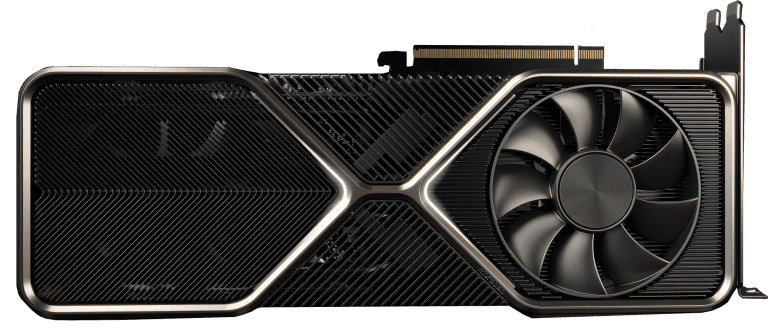
NVIDIA GeForce RTX 3070

Graphics Processor
GPU Name: GA104
GPU Variant: GA104-300-A1
Architecture: Ampere
Foundry: Samsung
Process Size: 8 nm
Transistors: 17,400 million
Die Size: 392 mm²
Graphics Card
Release Date: Sep 1st, 2020
Availability: Oct 29th, 2020
Generation: GeForce 30
Predecessor: GeForce 20
Successor: GeForce 40
Production: Active
Launch Price: $499 USD
Bus Interface: PCIe 4.0 x16
Clock Speeds
Base Clock: 1500 MHz
Boost Clock: 1725 MHz
Memory Clock: 1750 MHz, 14 Gbps effective
Memory
Memory Size: 8 GB
Memory Type: GDDR6
Memory Bus: 256 bit
Bandwidth: 448.0 GB/s
Board Design
Slot Width: Dual-slot
Length: 242 mm, 9.5 inches
Width: 112 mm, 4.4 inches
TDP: 220 W
Suggested PSU: 550 W
Outputs: 1x HDMI 2.1, 3x DisplayPort 1.4a
Power Connectors: 1x 12-pin
Board Number: PG142 SKU 10
Graphics Features
DirectX: 12 Ultimate (12_2)
OpenGL: 4.6
OpenCL: 3.0
Vulkan: 1.3
CUDA: 8.6
Shader Model: 6.6
Render Config
Shading Units: 5888
TMUs: 184
ROPs: 96
SM Count: 46
Tensor Cores: 184
RT Cores: 46
L1 Cache: 128 KB (per SM)
L2 Cache: 4 MB
Theoretical Performance
Pixel Rate: 165.6 GPixel/s
Texture Rate: 317.4 GTexel/s
FP16 (half) performance: 20.31 TFLOPS (1:1)
FP32 (float) performance: 20.31 TFLOPS
FP64 (double) performance: 317.4 GFLOPS (1:64)
NVIDIA GeForce RTX 4070

Graphics Processor
GPU Name: AD104
GPU Variant: AD104
Architecture: Ada Lovelace
Foundry: TSMC
Process Size: 4 nm
Transistors: 35,800 million
Die Size: 295 mm²
Graphics Card
Release Date: 2022
Availability: 2022
Generation: GeForce 40
Predecessor: GeForce 30
Production: Unreleased
Bus Interface: PCIe 4.0 x16
Clock Speeds
Base Clock: 2310 MHz
Boost Clock: 2610 MHz
Memory Clock: 1325 MHz, 21.2 Gbps effective
Memory
Memory Size: 12 GB
Memory Type: GDDR6X
Memory Bus: 192 bit
Bandwidth: 508.8 GB/s
Board Design
Slot Width: Dual-slot
Length: 336 mm, 13.2 inches
Width: 140 mm, 5.5 inches
Height: 61 mm, 2.4 inches
TDP: 285 W
Suggested PSU: 600 W
Outputs: 1x HDMI 2.1, 3x DisplayPort 1.4a
Power Connectors: 1x 12-pin
Board Number: PG141 SKU 331
Graphics Features
DirectX: 12 Ultimate (12_2)
OpenGL: 4.6
OpenCL: 3.0
Vulkan: 1.3
CUDA: 8.9
Shader Model: 6.6
Render Config
Shading Units: 7680
TMUs: 240
ROPs: 80
SM Count: 60
Tensor Cores: 240
RT Cores: 60
L1 Cache: 128 KB (per SM)
L2 Cache: 48 MB
Theoretical Performance
Pixel Rate: 208.8 GPixel/s
Texture Rate: 626.4 GTexel/s
FP16 (half) performance: 40.09 TFLOPS (1:1)
FP32 (float) performance: 40.09 TFLOPS
FP64 (double) performance: 626.4 GFLOPS (1:64)
To conclude...
The xx70 series of graphics cards have improved quite a bit since their first iteration. They are a good value GPU, providing quality gaming at a reasonable price. If you’re looking for a card that gives you a bang for your buck, the xx70 cards are a good starting point.


Recent Comments